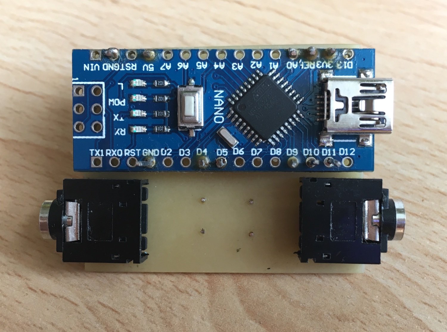
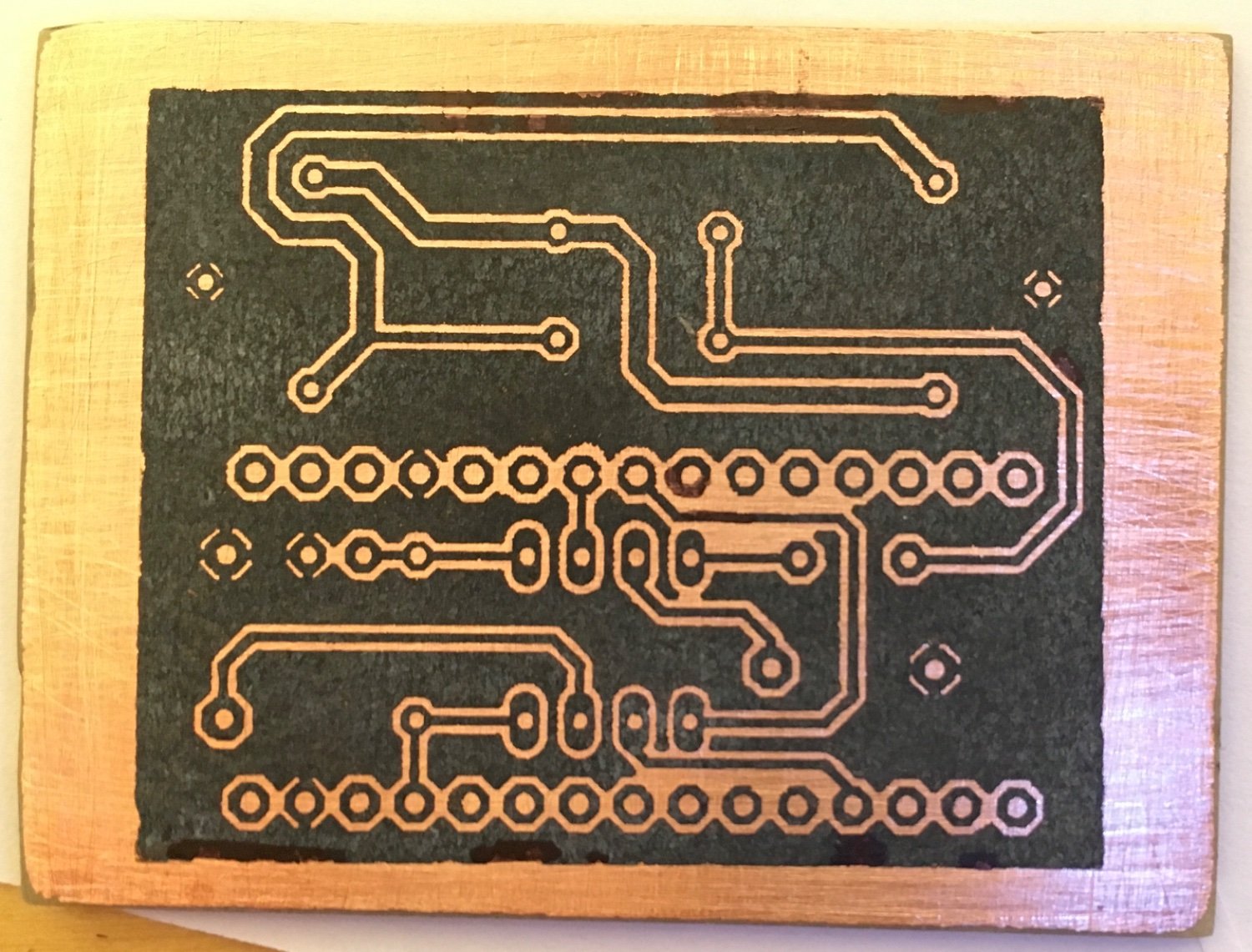
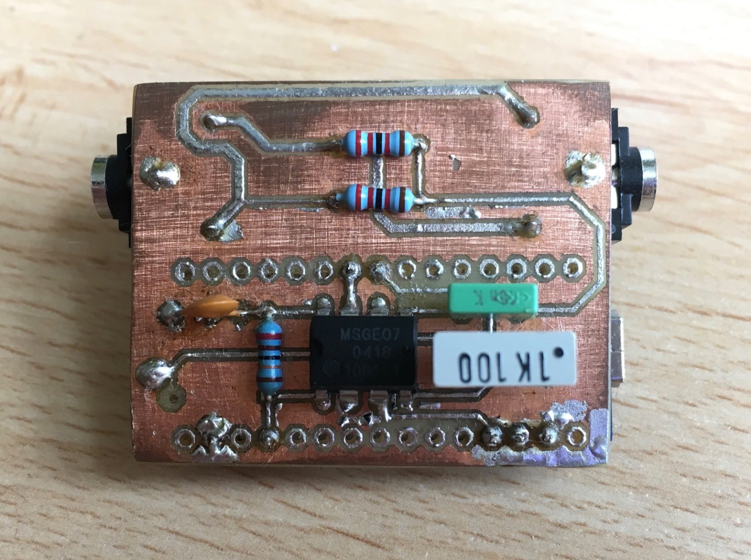
This was my first try developing my own pcb with the toner transfer method. I did this project many years back but it works perfectly to this day.
It filters an audio signal and drives led strips so they pulsate to the beat of a song.
Projects, pictures, industry discussions and news about electronic engineering & component-level electronic circuits.
1: Be nice.
2: Be on-topic (eg: Electronic, not electrical).
3: No commercial stuff, buying, selling or valuations.
4: No circuit design or repair, tools or component questions.
5: No excessively promoting your own sites, social media, videos etc.
Ask questions in https://discuss.tchncs.de/c/askelectronics
This was my first try developing my own pcb with the toner transfer method. I did this project many years back but it works perfectly to this day.
It filters an audio signal and drives led strips so they pulsate to the beat of a song.
Nicely done. I have given up on toner transfer and instead use a laser attached to a 3D printer to burn away spraypaint.
Alignment on double sided boards is difficult though.
Interesting, how much power does the laser have to need to be able to burn the paint?
I'm using a 10W laser at about 25% of its power. It's a 450nm laser that is sold as 80W electrical power on AliExpress but Chinese webshops often exaggerate their specs.
Is this one of those IYKYK or is there further explanation of the process involved?
Sounds amazing and fascinating but I have no idea how it's accomplished.
I’m assuming you’re not super familiar with PCB fabrication? The toner transfer is a way to get small, repeatable, and precise definition of the component pads and traces - at home - without needing the expensive industrial machinery that fab houses have.
The toner ’print’ is a negative image, placed on a sheet of copper mounted to (usually) fiberglass. Much like masking off areas when painting, the ‘print’ protects the copper surface in select areas you want to keep safe when the whole board goes into the acid bath to dissolve the unprotected copper - leaving copper only where your ‘print’ was, and hopefully no shorts/grounds.
Definitely cool to have the ability to DIY fine pitch if you’re manually mounting SMT components or want higher board density, beats out the hand drawn permanent marker lines I’ve done in the past 😅
That's a really nice project, I often thought of trying to do my own board to move project from breadboard to something permanent, and never got the motivation high enough to do it. So congratulations on your realization.
I must add, as a certified ipc-610 trainer that board gives me goose bumps, the Halloween kinds. (I'm just a professional critic, my projects are way, way worst)
Haha, the board won‘t win any prices for sure. But for a first try I‘m still very happy.
It's just the soldering. A drop of flux make wonders. The pwb is very decent, impressive even. You can be happy.