You can do all sorts of nifty things when you're designing silicon. Including this abomination.
https://en.wikipedia.org/wiki/Carcinisation
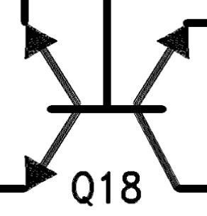
Source: datasheet for LM161, a high speed (20ns delay) moderately high voltage (30V) comparator. I'm going to try and make a discrete version of some bits of it and see how well it works. Maybe not this triple-emitter NPN though, I draw the line at components that require livestock sacrifices.
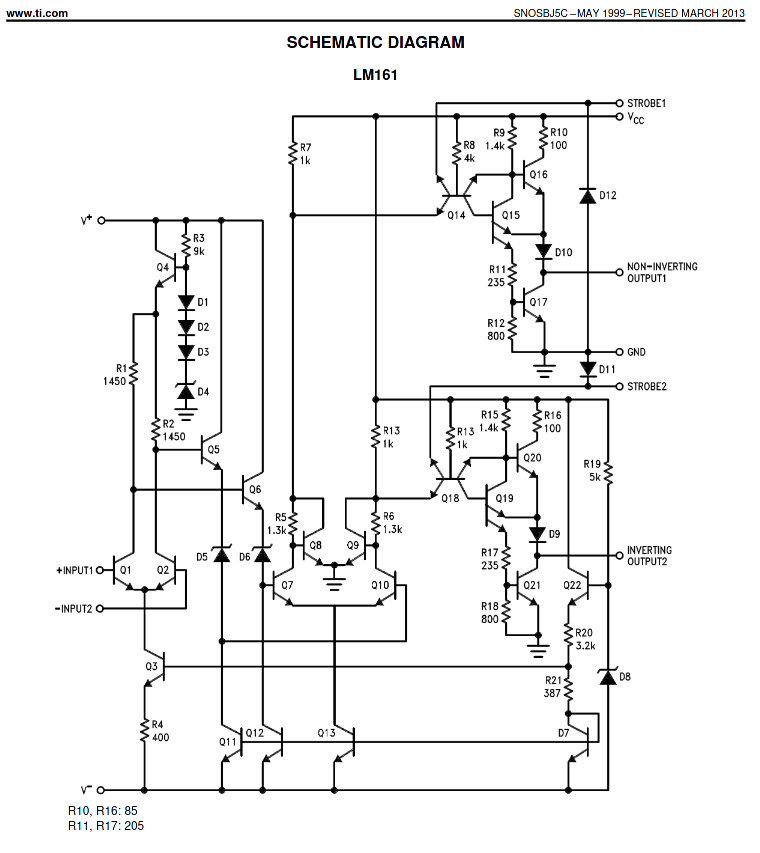
That Wiki page is woefully incomplete, only covering the digital applications (and these days digital stuff is all done with FETs, not BJTs). Camenzind's Designing Analog Chips has quite a bit more info.
It's hard to control the exact area of the emitter diffusion in a BJT. Think of how an NPN transistor is made on an IC: there's some substrate that the collector gets connected to, then an area is masked off & the unmasked area is doped enough to make it a P-type silicon region. That doping process will have some variation in depth & the masking is never perfect, some will diffuse a bit past the edges of the mask, or not enough will diffuse in. Then another mask layer is applied, and N-dopant is added in the open space to form the emitter. That's also imperfect, on top of an already imperfect base. So the exact gain of transistors isn't well-controlled, even for a very well-controlled collector voltage.
Instead, IC makers can dope multiple smaller emitters in a bigger base region. Smaller doped regions are easier to control (less time for over-diffusion of the dopant) and having a bunch of them has an extra advantage: you can match the ratio of collectors to emitters from one transistor to the ratio of collectors to emitters of another, and variations in the area of any individual emitter will be a much smaller percentage of the total error since the errors of the different emitters will tend to cancel out.
Also, the high-current capability of a BJT is controlled by the emitter length, not the emitter area. Splitting an emitter into long strips can increase how much current a transistor can handle.
Similar things apply to the collector.
For SPICE modeling or building discrete versions of ICs, use multiple transistors in parallel.